Week 3 - Electronics Design
Assignments of the Week
- Use an EDA tool to design a development board that uses parts from the inventory to interact and communicate with an embedded microcontroller
- Extra credit: try another design workflow
- Extra credit: simulate your design
- Extra credit: design a case around your design
For this week's project, I am focusing on developing a custom expansion board based on the Seeed Studio XIAO ESP32-C3 microcontroller. The board is specifically designed to integrate with A4988 stepper motor drivers, providing precise motor control capabilities. This comprehensive PCB design process encompasses everything from component selection and schematic creation to PCB layout optimization and manufacturing file generation, ensuring both functionality and manufacturability of the final product.
PCB Design Process
1.Project Initialization
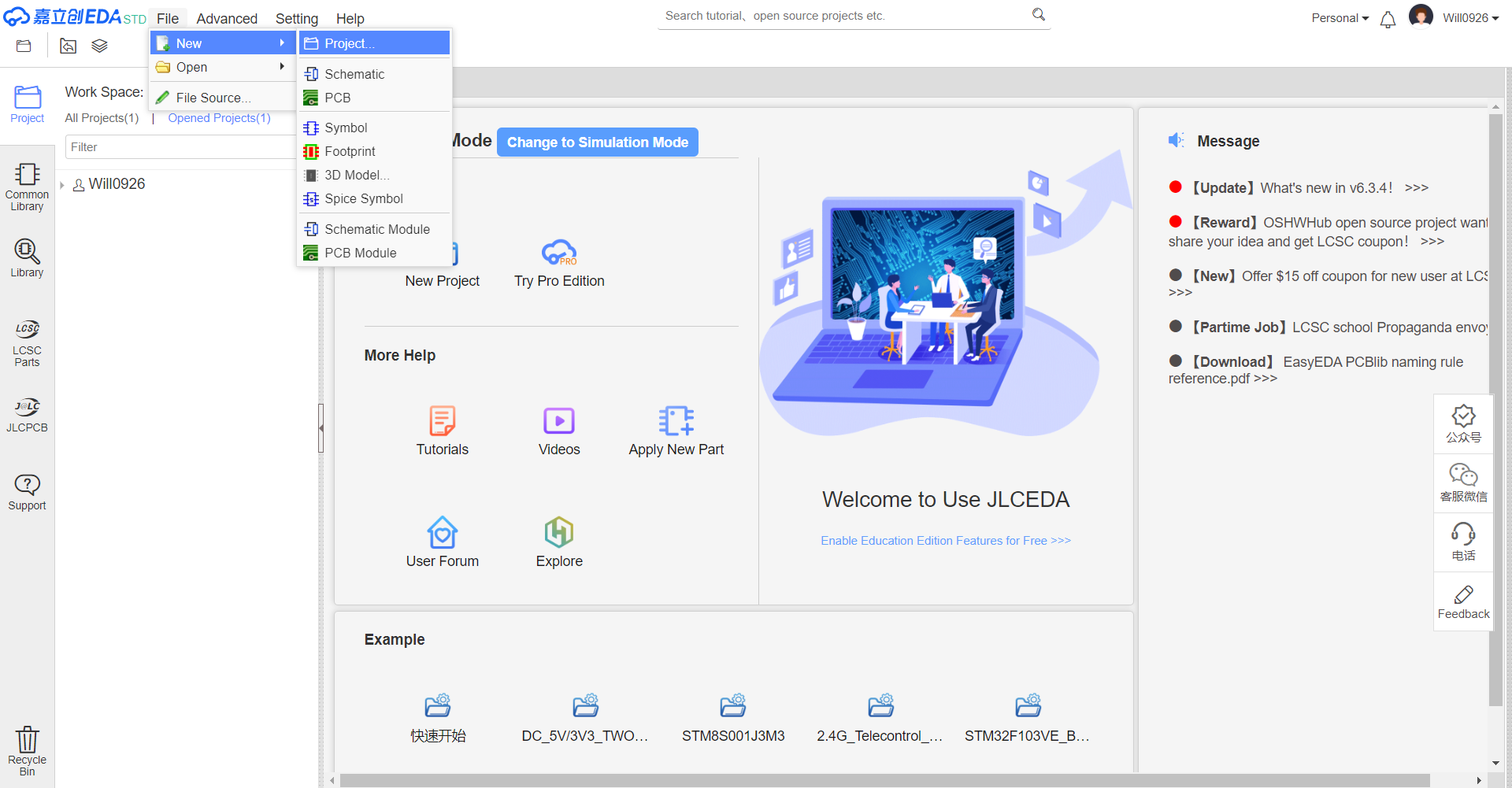
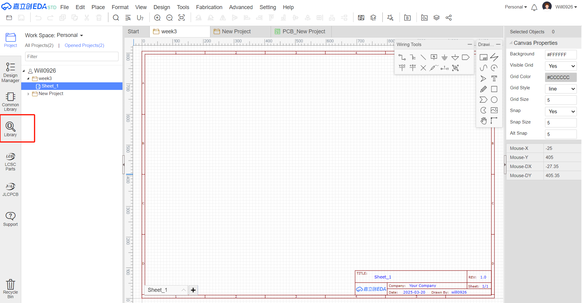
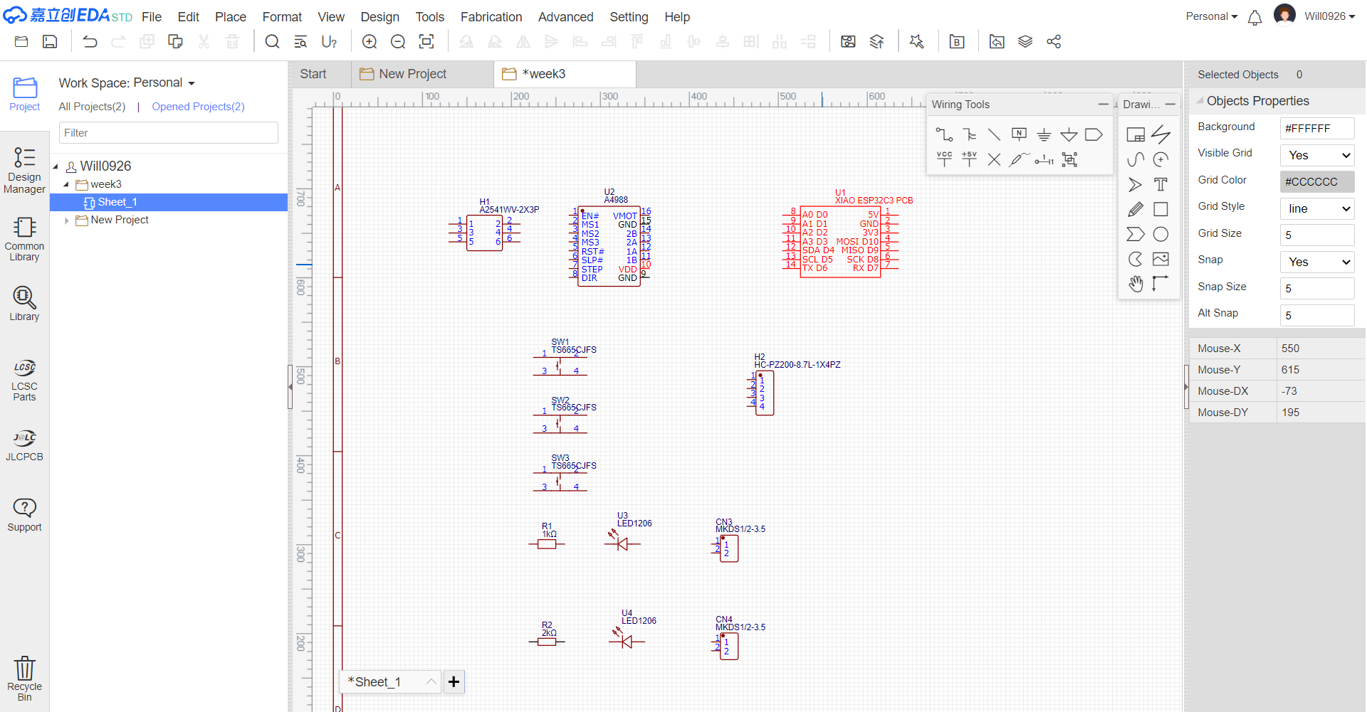
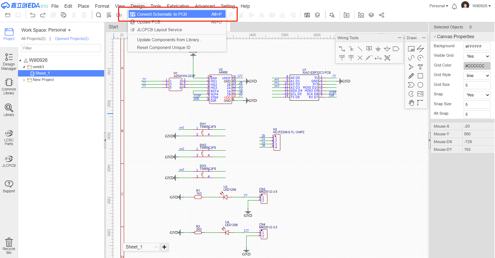
Create a new electronic design project in LCEDA:
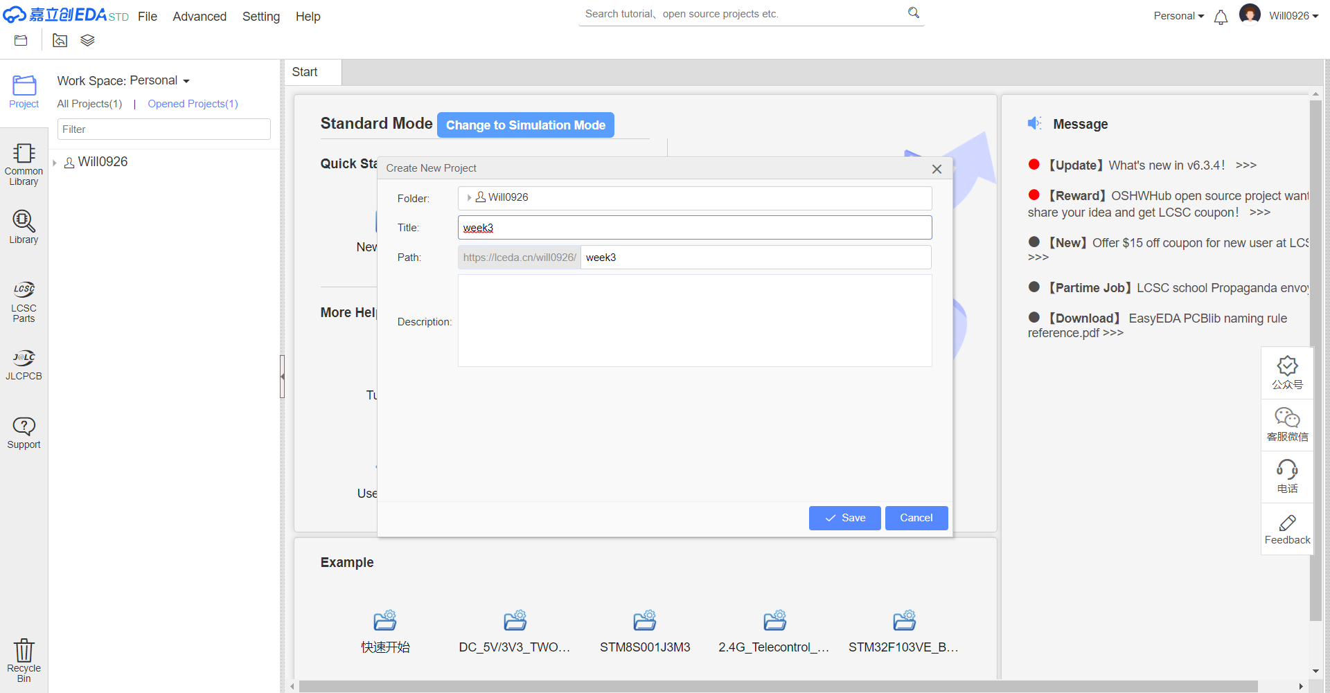
- Create a new project and select "project"
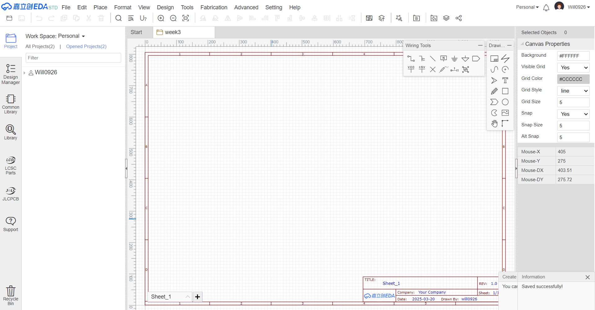
- Select "Save", then a new project is created.
2.Component Library Preparation
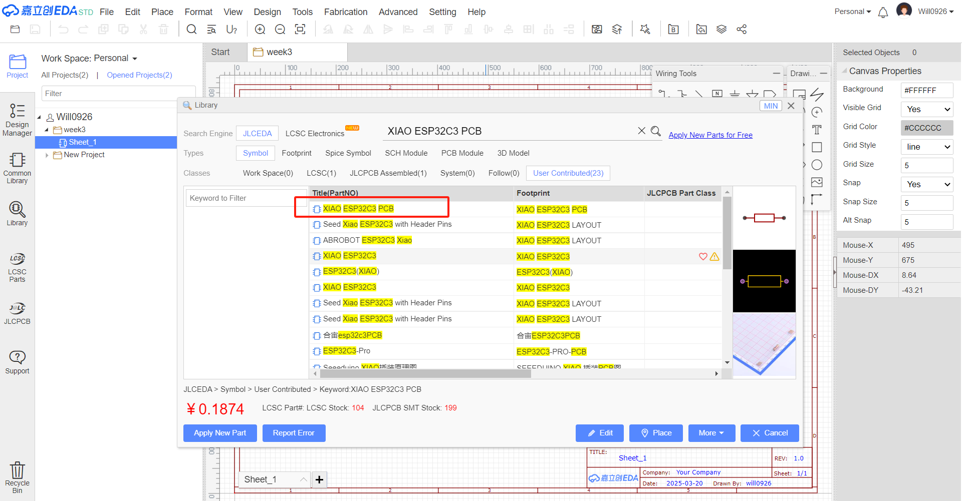
In LCEDA, I need to use component models for the Seeed Studio Xiao ESP32-C3 and A4988 stepper motor driver.
- Click on "Library", then enter "XIAO ESP32C3 PCB" in the search bar, and you will find "XIAO ESP32C3 PCB", and then double click it.
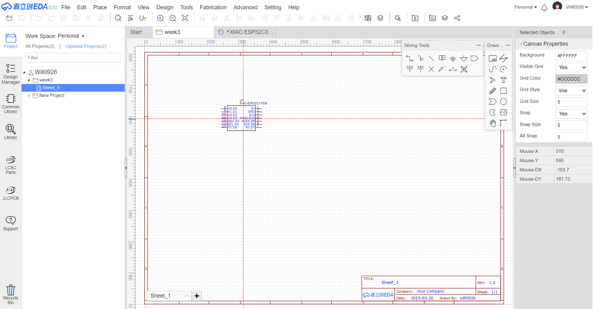
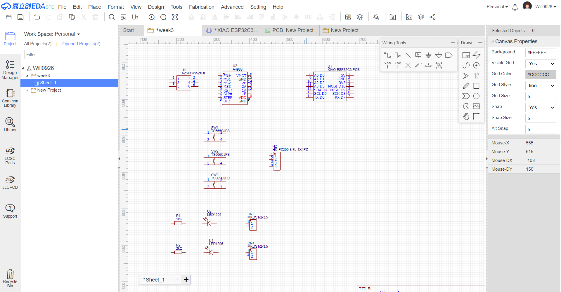
3.Place A4988 and other modules in the schematic using the same method
3.Hardware Specification Analysis
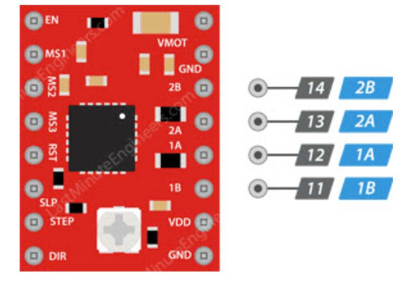
3.1Pin Definitions
Below are the pin definitions for XIAO ESP32-C3 and A4988. Based on these definitions, I can connect four A4988 modules to the XIAO ESP32-C3 to achieve independent control of four stepper motors. 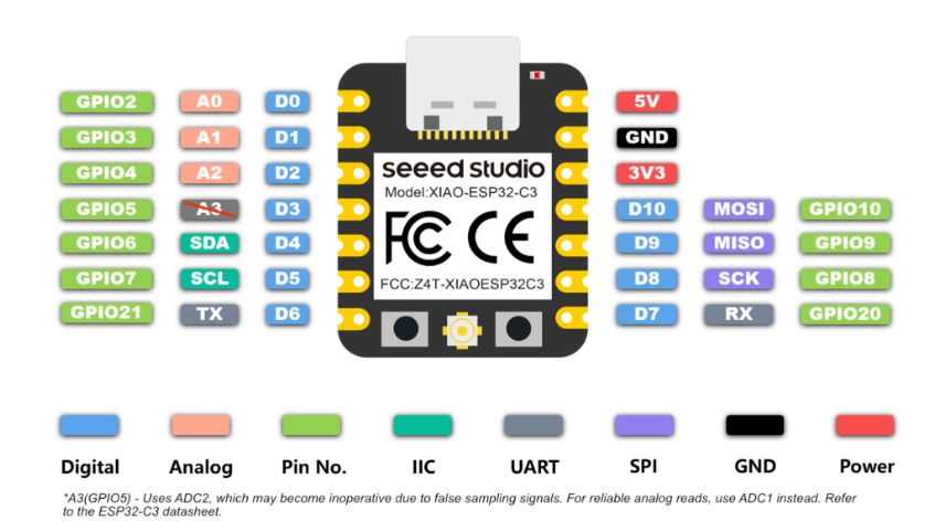
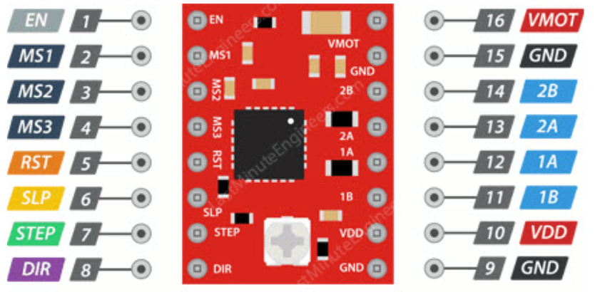
3.2 A4988 Technical Specifications
Here are the technical specifications for the A4988:
| Parameter Type | Specification |
|---|---|
| Motor Output Voltage | 8V – 35V |
| Logic Input Voltage | 3V – 5.5V |
| Continuous Current per Phase | 1A |
| Maximum Current per Phase | 2A |
| Microstepping Resolution | Full, 1/2, 1/4, 1/8, 1/16 |
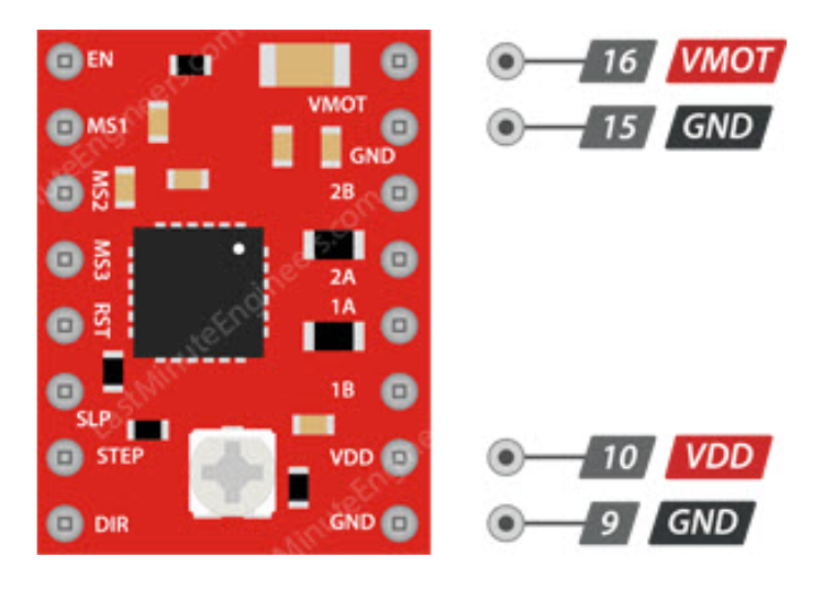
3.3Power System
A4988 requires two power connections:
- Logic Power VDD-GND: 3V-5.5V, for internal logic circuits
- Motor Power VMOT-GND: 8V-35V, for motor drive
- Note: Motor power requires decoupling capacitors to maintain current
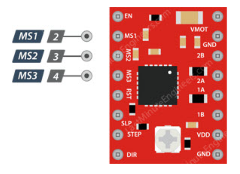
3.4Microstepping Control
The A4988 driver supports microstepping, which achieves finer step divisions by applying intermediate current levels to the motor coils.
- MS1/MS2/MS3: Used to select microstepping resolution, different logic level combinations can set different microstepping modes.
- Default state: Pulled down to full-step mode. For example, when driving a NEMA 17 motor (1.8° step angle, i.e., 200 steps/revolution) in quarter-step mode, the motor will execute 800 microsteps per revolution.
3.5Motion Control
A4988 has two control input pins - STEP and DIR.
- STEP: Step control, each high-level pulse sent to this pin drives the motor according to the microstep selection pins. The faster the pulses, the faster the motor rotates.
- DIR: Direction control, high level for clockwise, low level for counterclockwise.
3.6Power Management
- EN: Enable control, default active-low input for this pin
- SLP: Sleep mode, enters on low level
- RST: Reset control, resets on low level
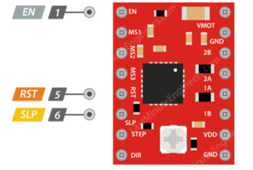
3.7Motor Output
- 1A/1B/2A/2B: Motor phase interfaces for connecting stepper motors.
4.Pin Assignment Plan
Below is the pin connection plan:
| Parameter Type | Specification |
|---|---|
| D0 | Motor 1 STEP |
| D1 | Motor 1 DIR |
| D2 | Motor 2 STEP |
| D3 | Motor 2 DIR |
| D4 | Motor 3 STEP |
| D5 | Motor 3 DIR |
| D6 | Motor 4 STEP |
| D7 | Motor 4 DIR |
| GND | All A4988 ENABLE |
| GND | All A4988 GND |
| 5V | All A4988 VDD |
5.Circuit Design Implementation
5.1Schematic Design
- Component Placement Open your existing schematic in LCEDA. Search for the symbols of switches, resistors, and diodes in the component library. If the required components are not in the library, you need to create custom symbols for them. Drag and drop the new components onto the schematic canvas.
- Pin Connections Connect the pins of these new components to other existing components in the schematic, such as the XIAO ESP32-C3, A4988 driver, or other related parts.
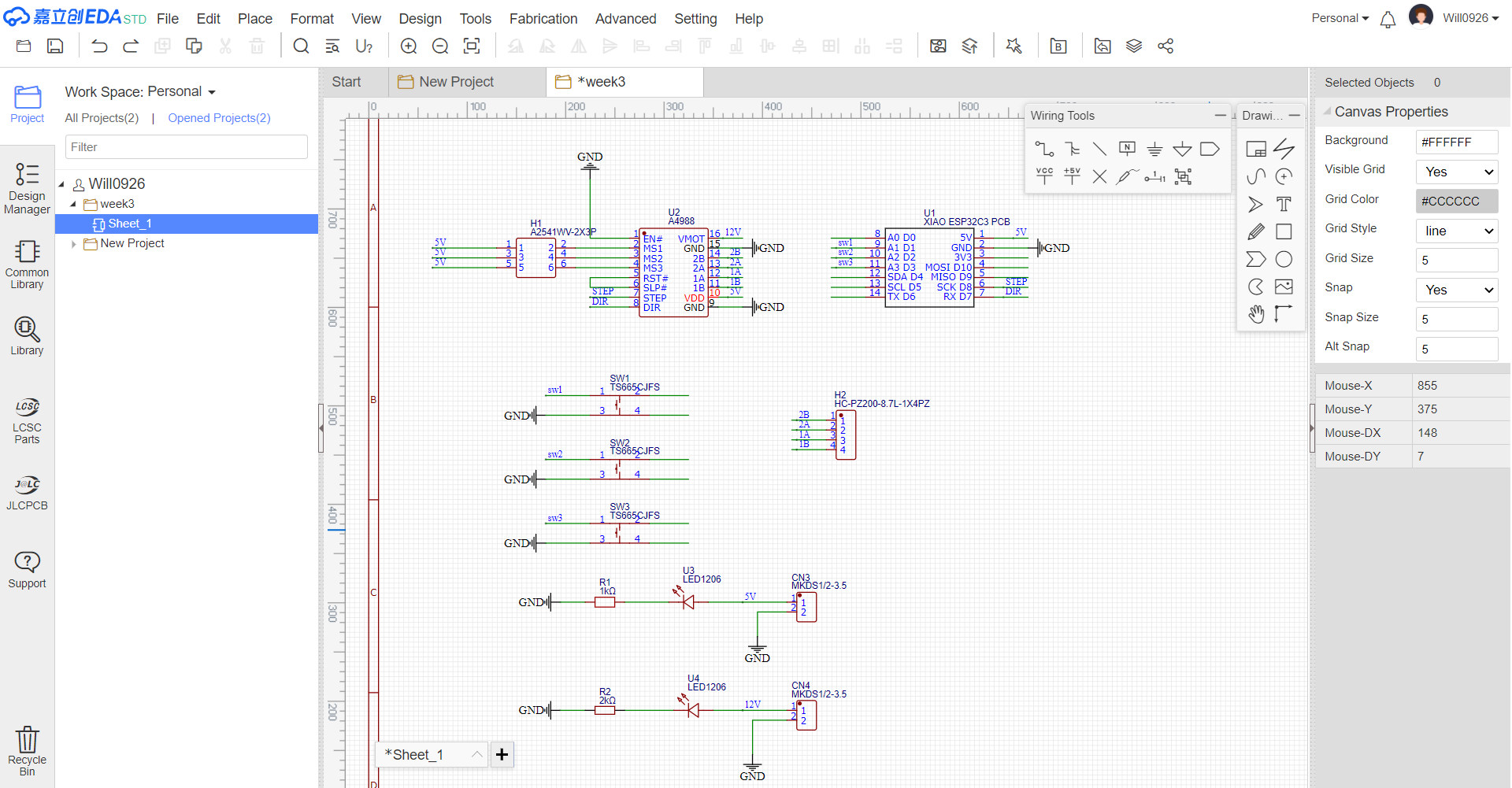
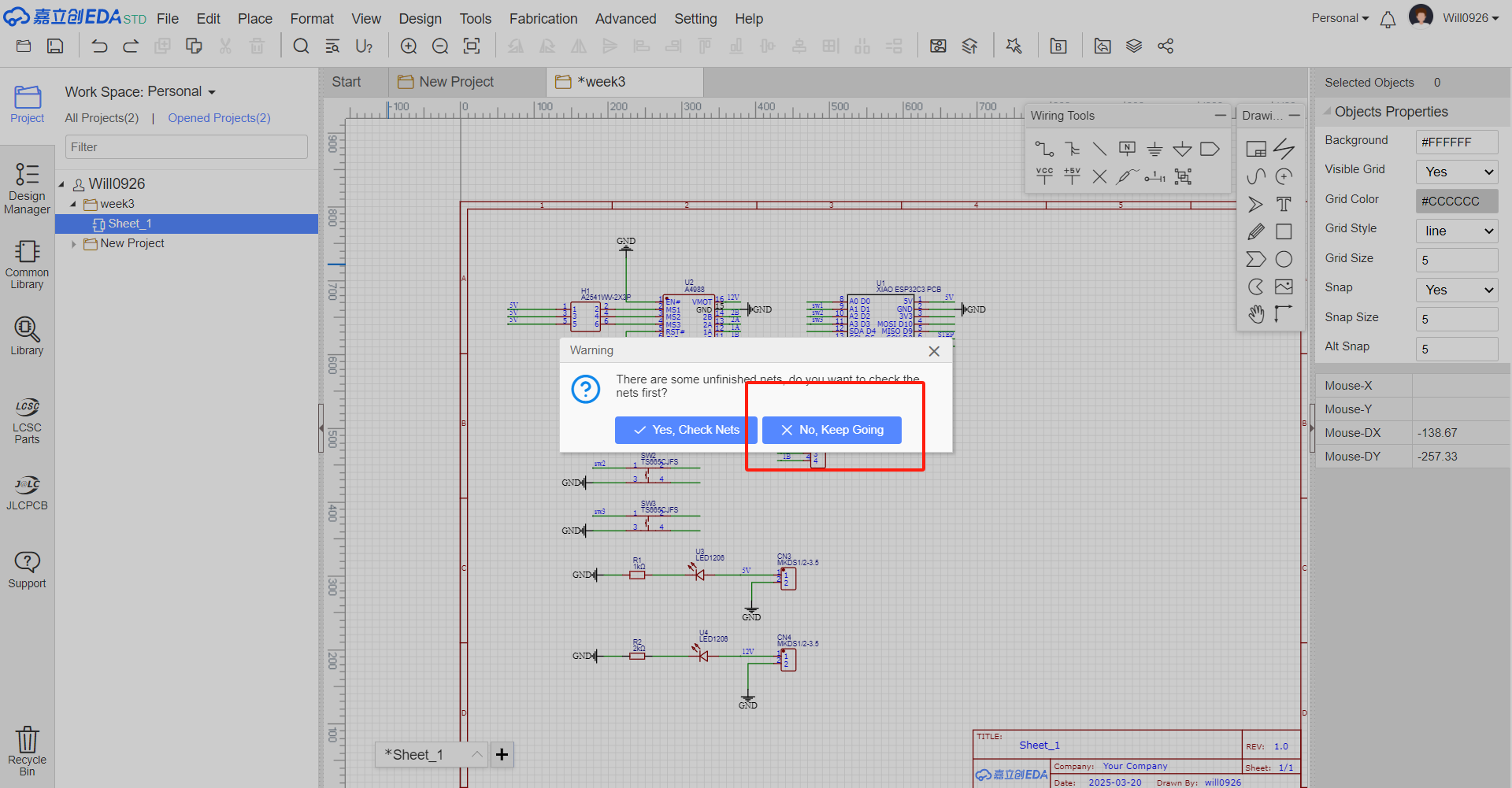
- Schematic Review Check the updated schematic for any incorrect connections, short-circuits, or missing connections. Use the error-checking tools in LCEDA to identify and fix potential issues.
5.2PCB Design Update
Generate PCB from Updated Schematic After finalizing the schematic with the new components, use LCEDA's function to transfer the updated schematic information to the PCB design area.
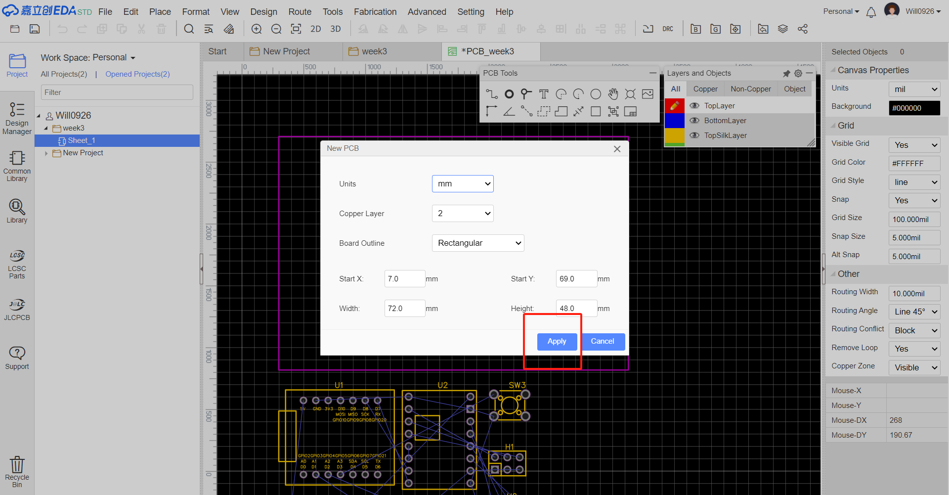
Component Placement on PCB Place the newly added switches and resistors on the PCB layout. Consider factors such as signal integrity, heat dissipation, and ease of assembly. Ensure that there is enough space for the new components and that they do not interfere with the existing components.
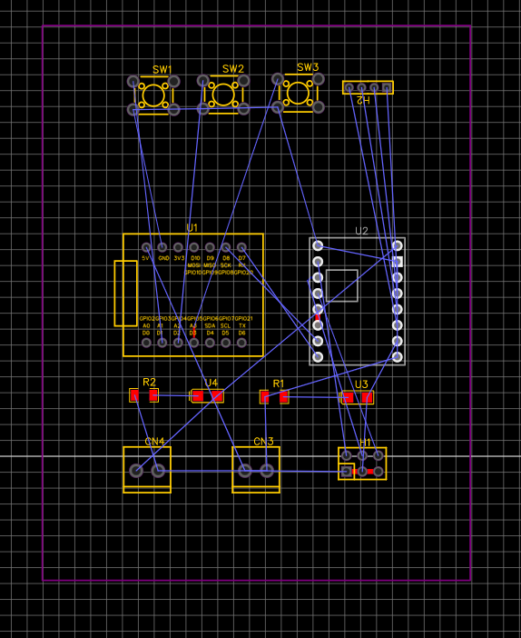
Routing Traces Route the electrical connections (traces) between the new component pins and other related pins on the PCB. Follow the design rules for trace width, spacing, and layer usage. For example, make sure that power traces for resistors are wide enough to handle the current. Here, we choose 5V line width 0.8mm, 12V line width 1.6mm, other line width 0.3mm
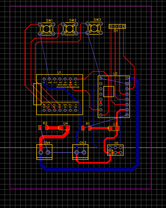
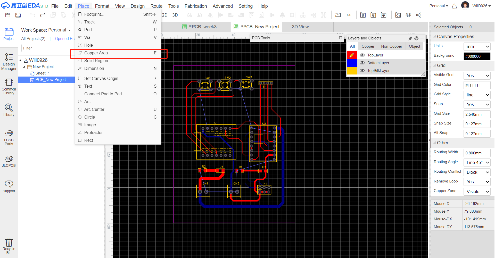
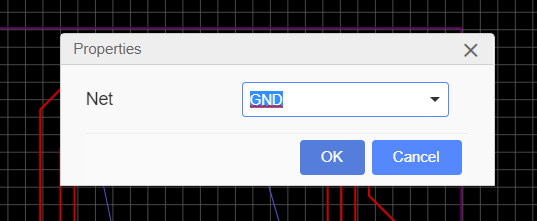
Ground connection Connect all ground interfaces with the "Copper Area" function.
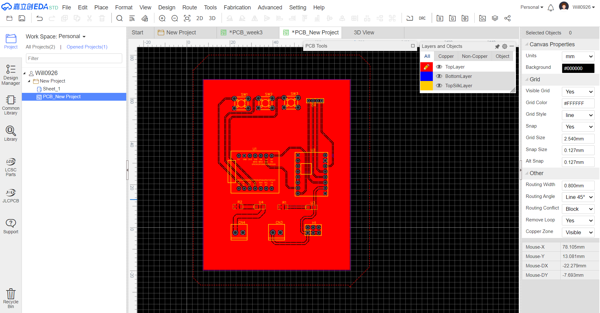
PCB Design Review Conduct a Design Rule Check (DRC) on the updated PCB design. Check for any violations of trace-to-trace clearance, hole size, and component-to-component spacing.
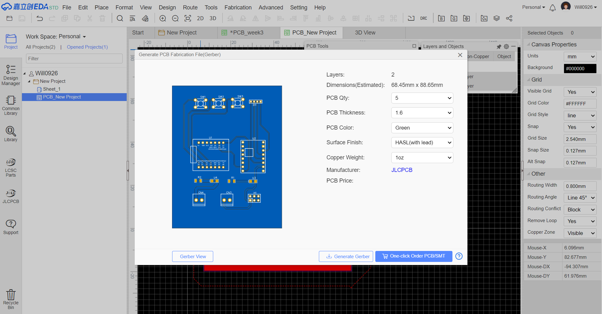
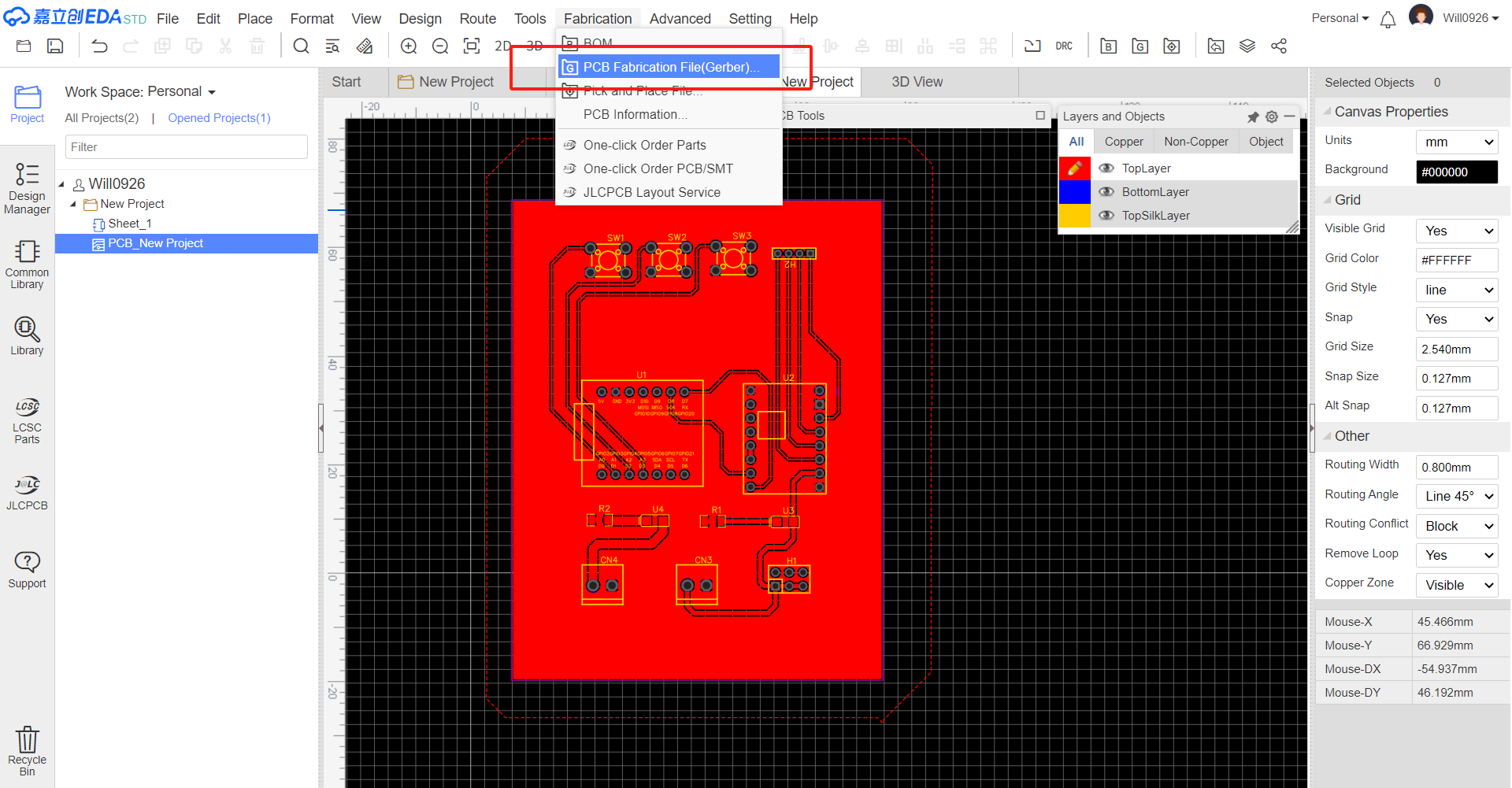
5.3 Generating Manufacturing Files
Export Gerber Files Use LCEDA's export function to generate the Gerber files for the updated PCB design. These files will be sent to the PCB manufacturer for production.
Update the Bill of Materials (BOM) Update the BOM to include the new components. List their part numbers, values, and quantities accurately. This will help in the procurement of components.