Appearance
Electric Design
1. Basic study of electronic components
(1) Resistance: Resistance, in electricity, property of an electric circuit or part of a circuit that transforms electric energy into heat energy in opposing electric current. Resistance is often considered as localized in such devices as lamps, heaters, and resistors, in which it predominates, although it is characteristic of every part of a circuit, including connecting wires and electric transmission lines.
(2) Capacitance: Capacitance is the ability of an object to store electric charge. It is measured by the change in charge in response to a difference in electric potential, expressed as the ratio of those quantities. Commonly recognized are two closely related notions of capacitance: self capacitance and mutual capacitance.
(3) Inductor: An inductor, also called a coil, choke, or reactor, is a passive two-terminal electrical component that stores energy in a magnetic field when an electric current flows through it. An inductor typically consists of an insulated wire wound into a coil.
2. Electric design tools
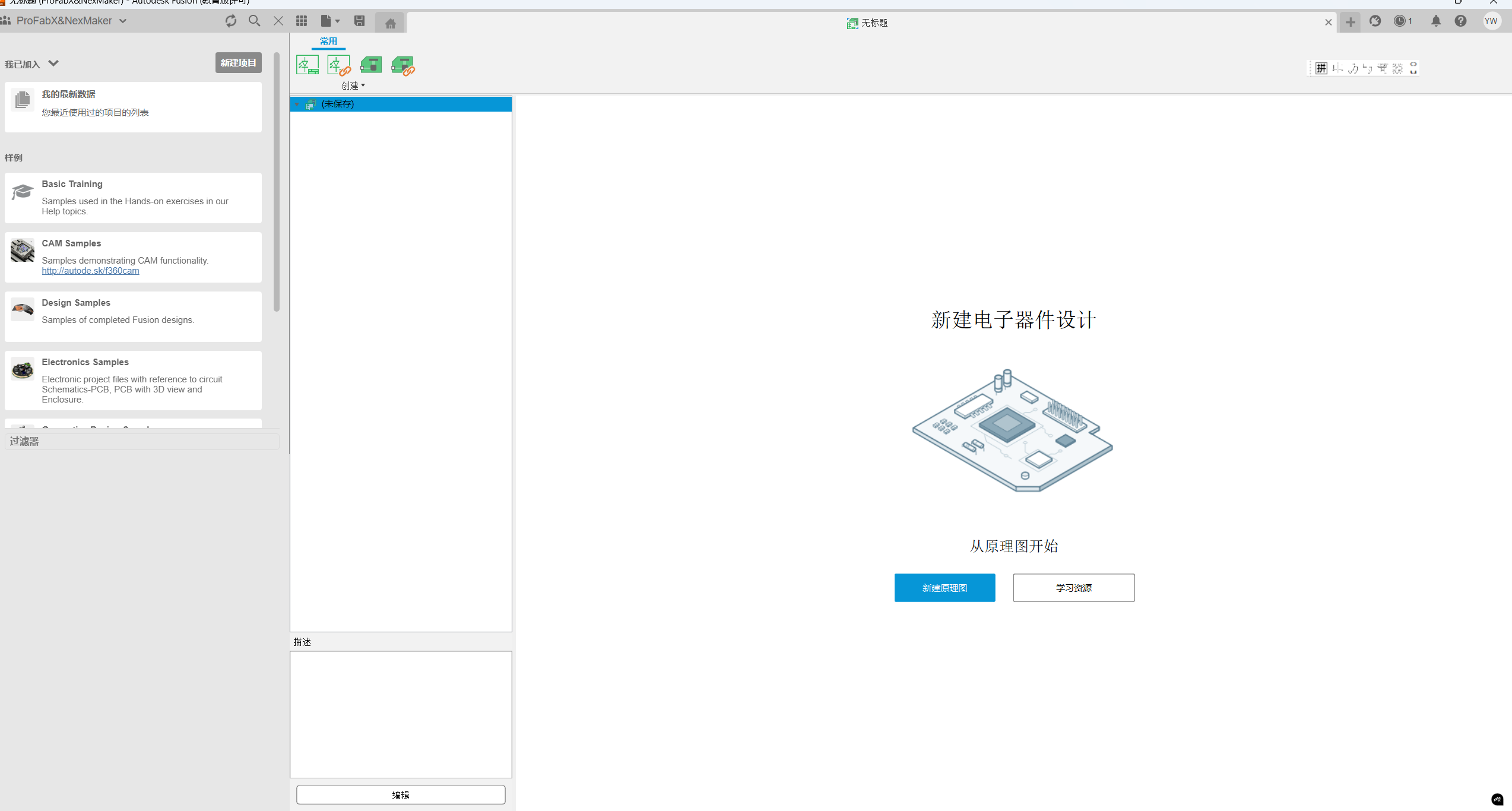
(1) Fusion: Fusion 360 is a 3D modeling and design software developed by Autodesk. It is widely used for creating 3D models of various objects, including mechanical, electrical, and computer parts. Fusion 360 allows users to create complex 3D models with ease, and it has a user-friendly interface that makes it easy to learn and use. 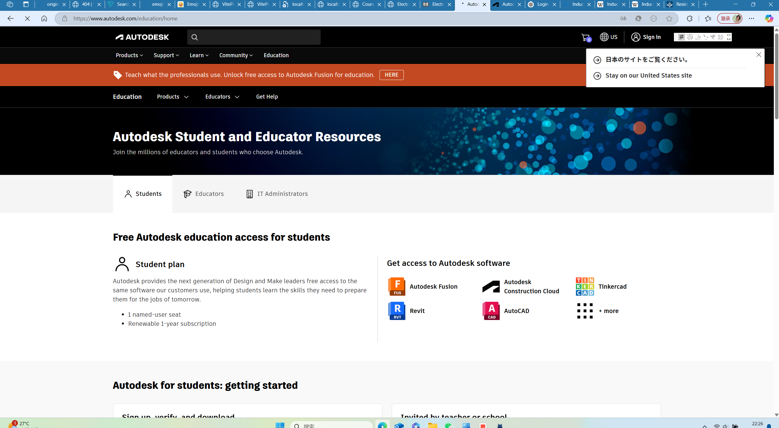
To download fusion, please click here. Then click Sign in for students.

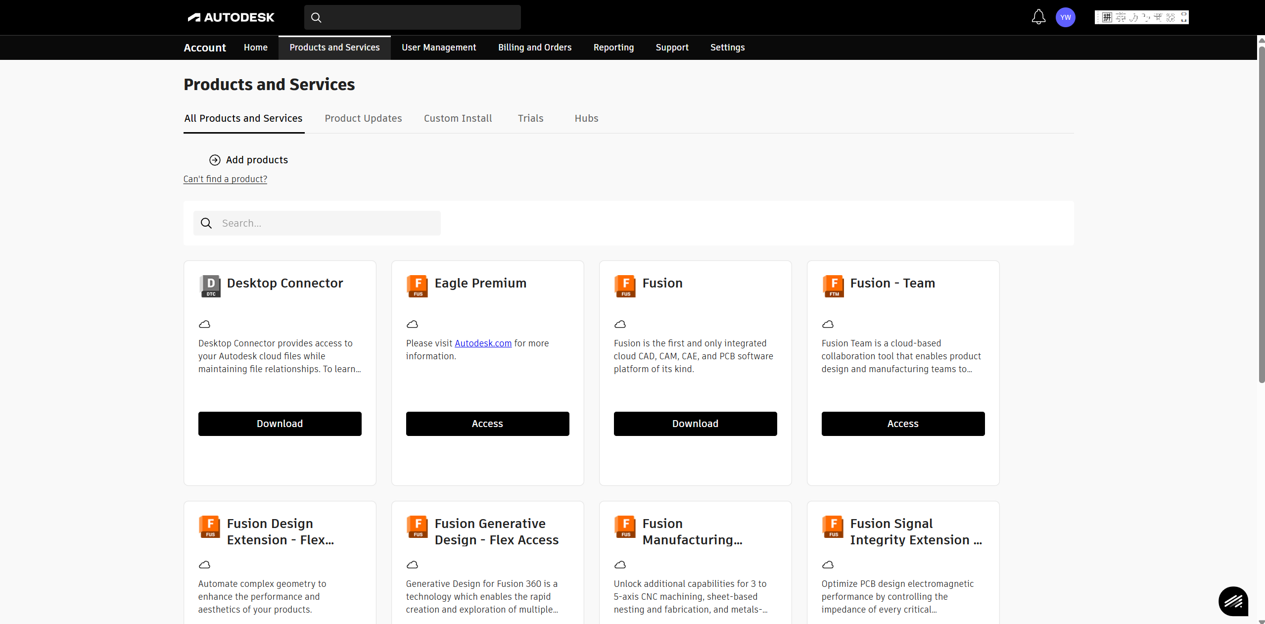
Tab the relevant information in this step.
Finally, download and install it.
To use the Fusion for electroc design. We need to install the nessessary libraries. Firstly, crease the schematic of circuit.
Then, click the libraries to find electric compoments.
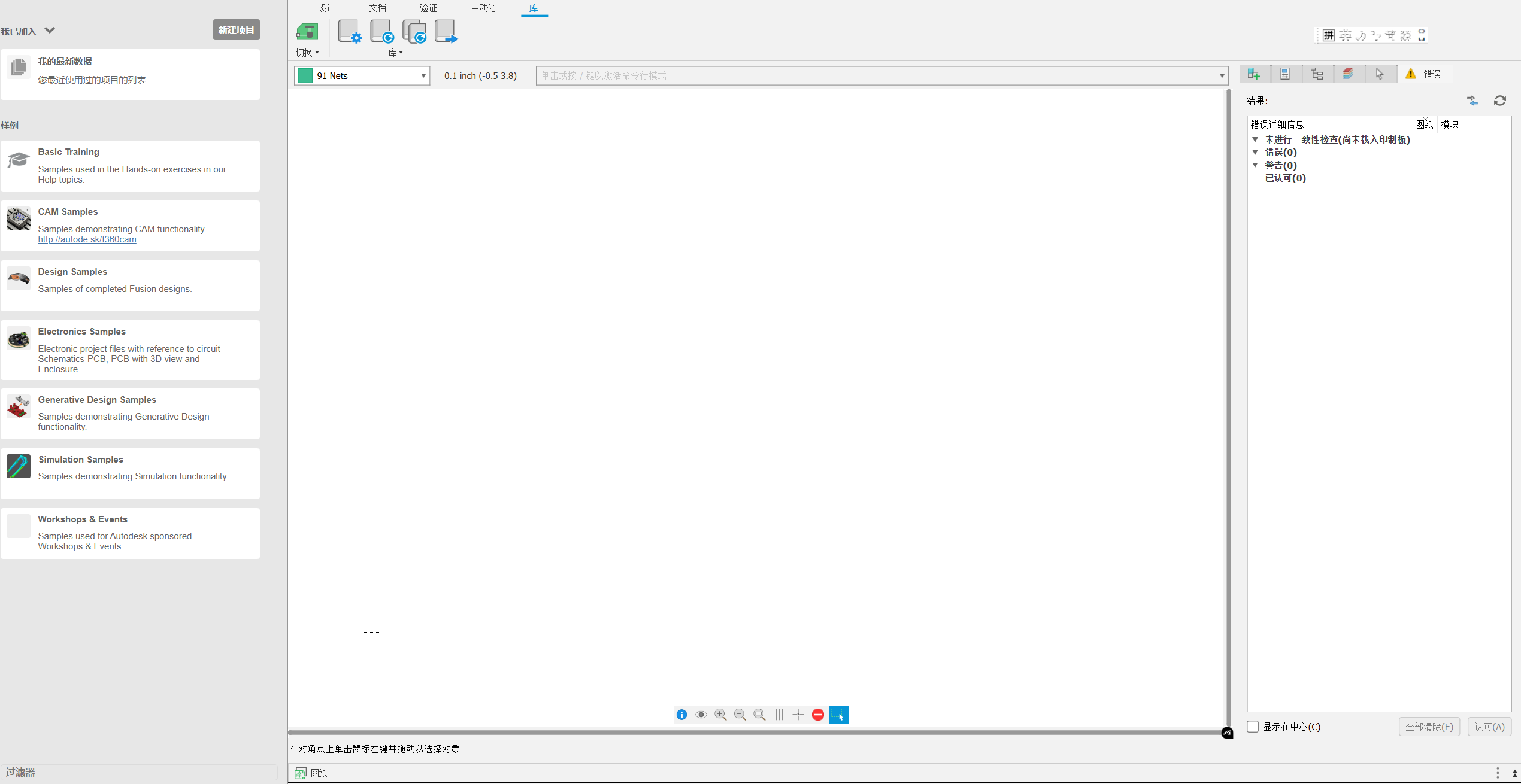
After clicking the libraries, the current pages show the Electronic component library.
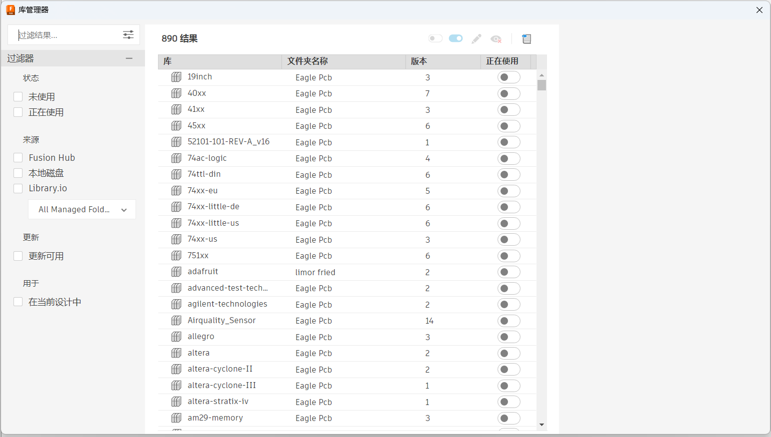
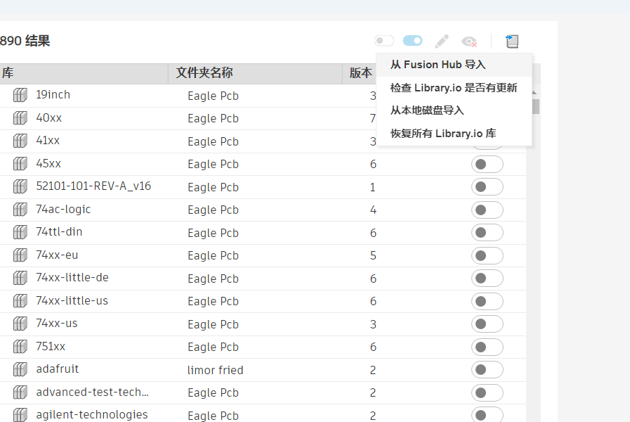
To manage the library, click the icon in the upper right corner and choose to add the libaray form local disk.
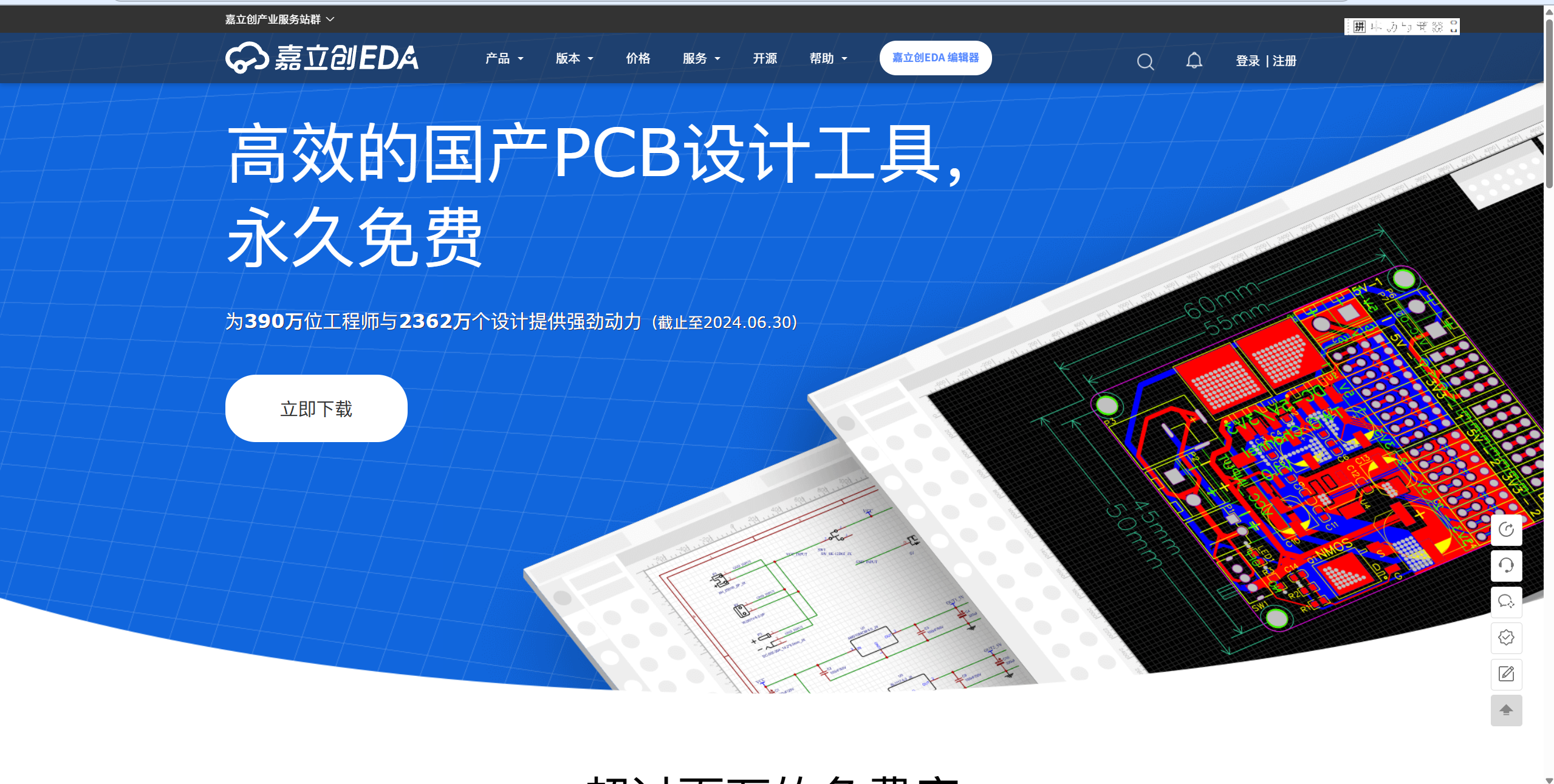
(2) JIALICHUANG eda: Jialichuang EDA is a browser-based, friendly and easy to use, powerful EDA (Electronics Design Automation: Electronic Design Automation) tool. This is the main page of Jialichuang EDA.After using this platform for electronic design, you can use the mall supported by this platform to place an order directly.
3. PCB borad design
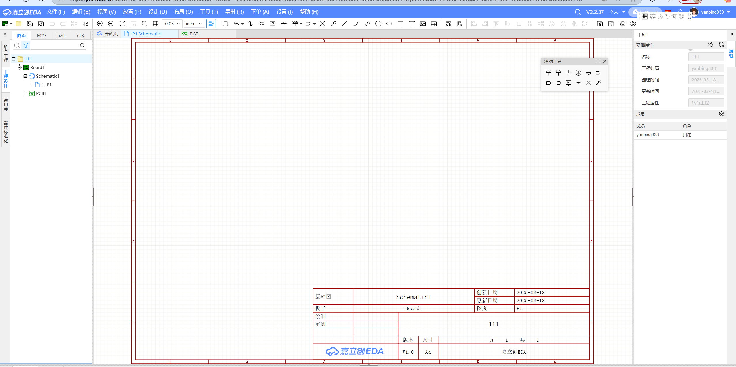
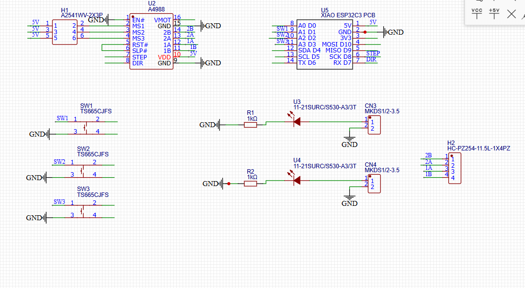
In this course, we will use JIALICHUANG EDA to design a PCB board. Firstly, add a new schematic.
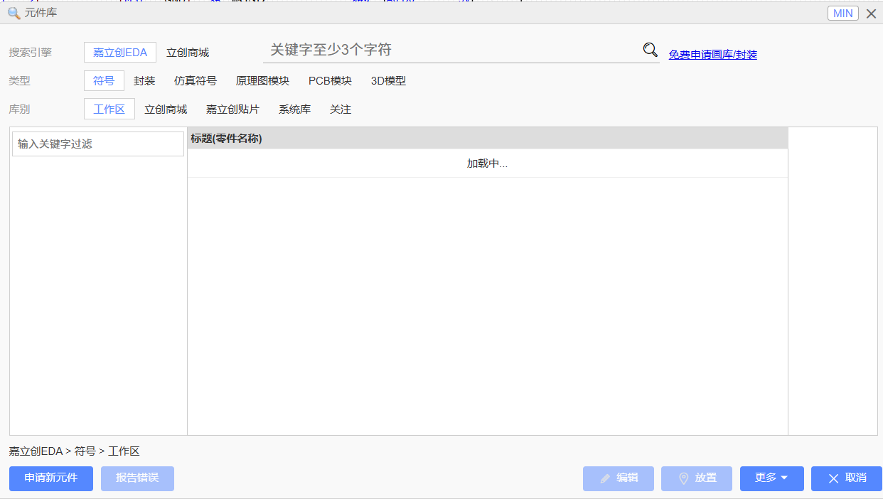
After that, we could add the electronic components to the schematic. The name of compoments could be found in the electronic component library.
By clicking the wire tool, the compoments were connected.
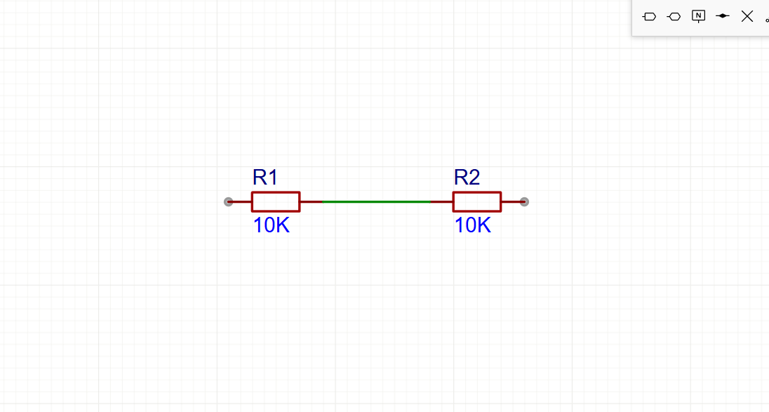
In the class, a simple PCB schamhematic was designed.
4. PCB board layout
To finish the PCB manufacturing, we should consider the layout of the PCB to make sure every wires are connected correctly, and all the PCB components are placed in the right place. In the same time, we should consider the function and real usingg scenario of the PCB boards, and make sure the PCB size is suitable.
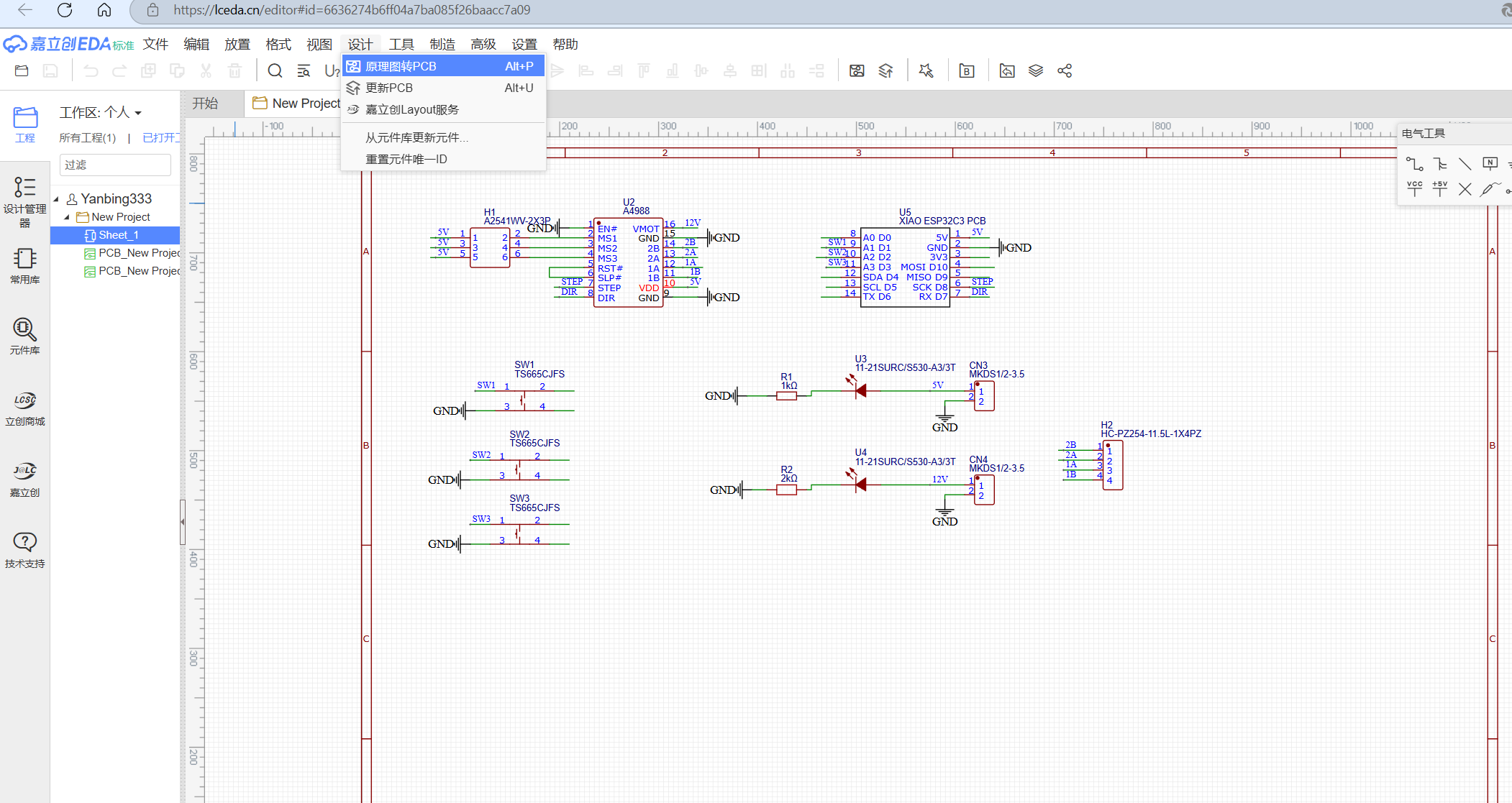
Firstly, we should convert the schmatic to PCB.
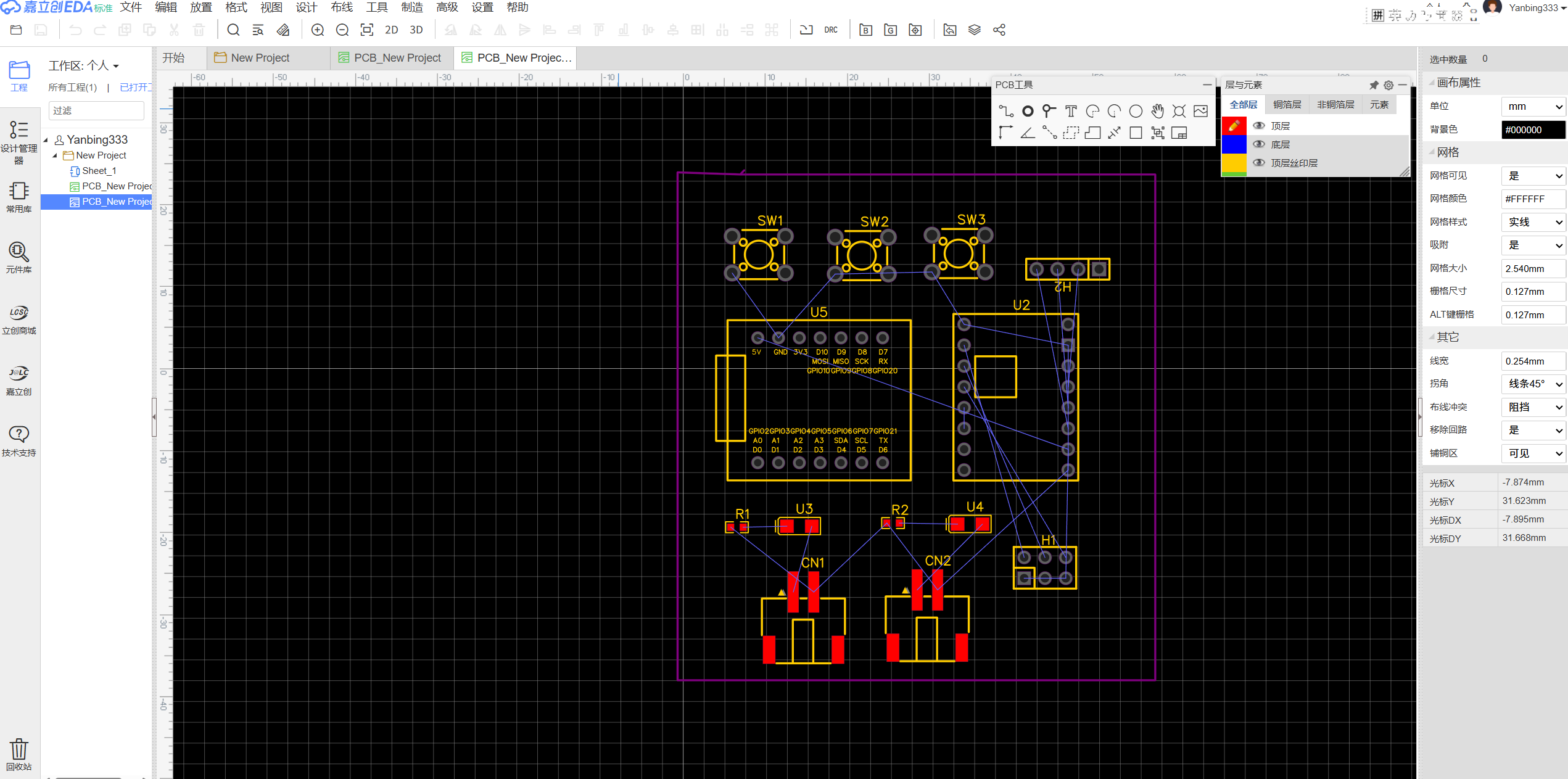
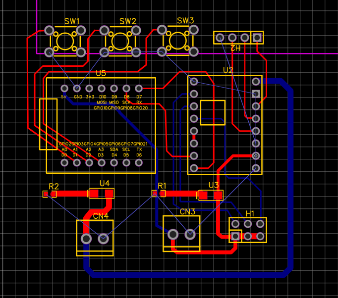
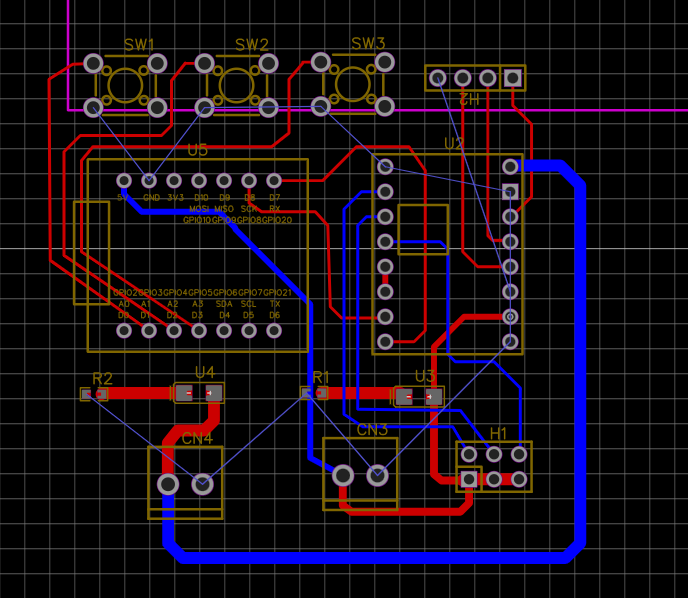
Then, we should arrange the place of the electric compoments and the wires of the PCB board. The wires are traces bend at 45° angles. One reason for this is that 45° angles shorten the electrical path between components compared to 90° angles. Another reason is that high speed logic signals can get reflected off the back of the angle, causing interference.

Larger circuits can be difficult to design on a single layer PCB. As design complexity increases, it gets harder to route the traces without intersecting one another. Luckily there are double, triple, and multi-layer PCBs that allow traces and planes to be routed on electrically isolated layers.
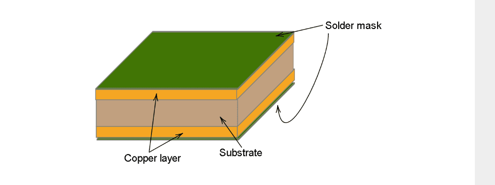
Double-layer PCBs have two copper layers, one on top and one on the bottom:
The first layer of the PCB board are arranged as the following figure.
The second layer of the PCB board are arranged as the following figure.
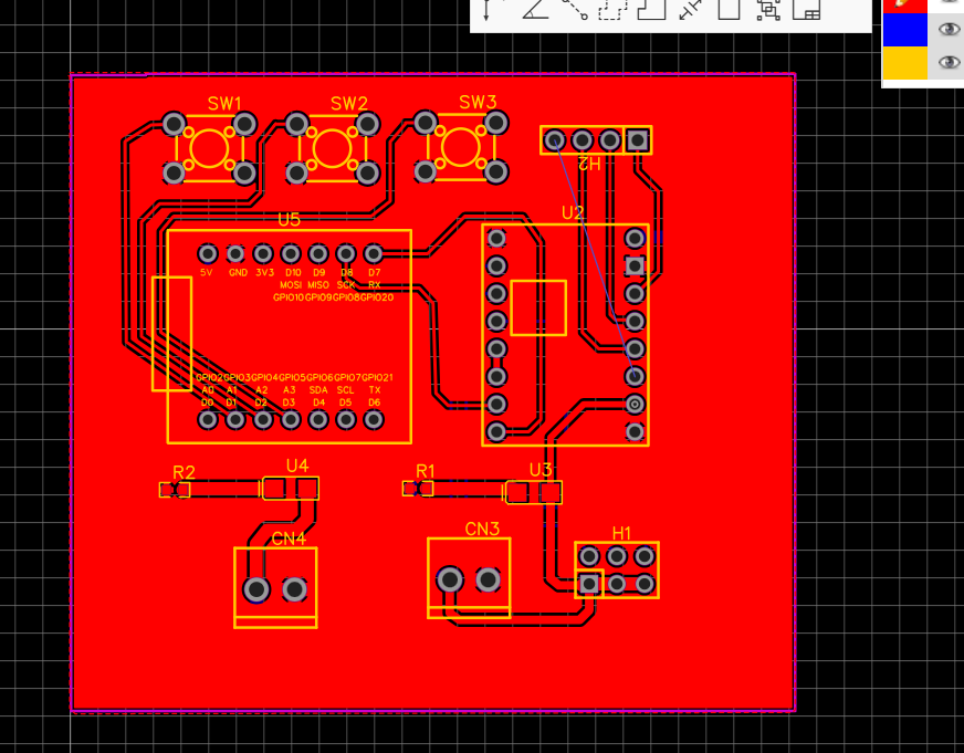
Finnaly, Copper plate laying of PCB. 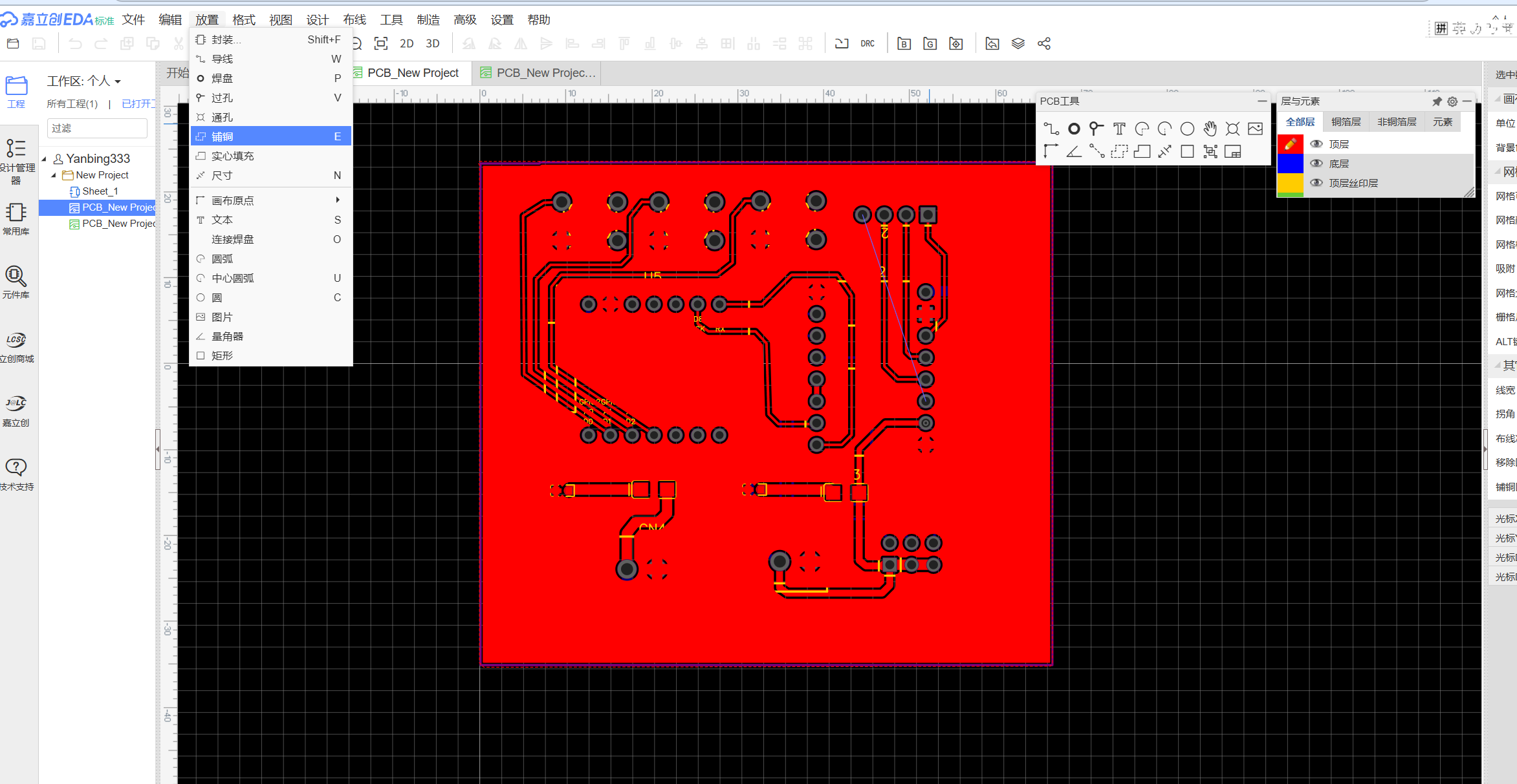
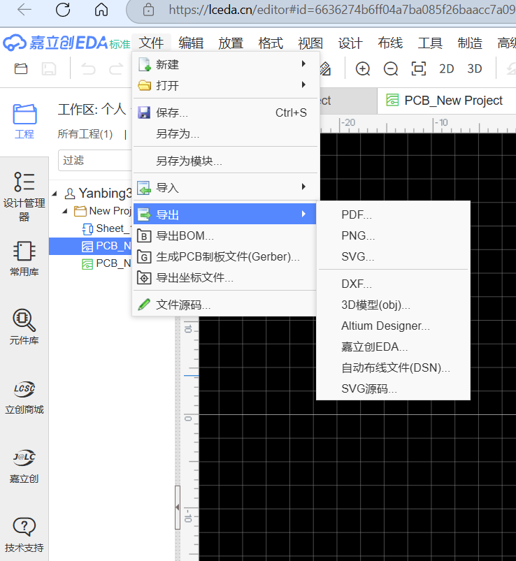
Finally, export the PCB design and send it to manufacturer.