PCB Design – Basic Knowledge and Tools
1. What is a PCB (Printed Circuit Board)?
A Printed Circuit Board (PCB) is a board used to mechanically support and electrically connect electronic components through conductive tracks, pads, and other features etched from copper sheets laminated onto a non‑conductive substrate. PCBs can range from simple 1‑layer boards to complex multi‑layer designs depending on the circuit complexity and application.
2. PCB Layers and Stackup
- Conductive Layers: Copper layers that carry electrical signals and power.
- Non‑conductive Layers: Solder mask, silkscreen/overlay, and other layers used for protection and labeling.
- Stackup refers to the order of layers in the PCB — e.g., 2‑layer, 4‑layer, 6‑layer boards.
3. Common PCB Components
- Pads: Copper areas where components are soldered (surface mount or thru‑hole).
- Vias: Plated holes connecting different layers (through vias, blind vias, buried vias).
- Traces: Copper pathways that connect components.
- Soldermask: Protective coating preventing shorts.
- Silkscreen/Overlay: Printed text and symbols used for assembly reference.
🕰️ Historical Context: The Vacuum Tube Era & Cold War Divergence
Before the dominance of PCBs and silicon transistors, the world of electronics was ruled by Vacuum Tubes (Valves). While the West raced to replace them, the Soviet Union refined them to their absolute peak.
Soviet vs. American Philosophies: A Technological Fork
During the Cold War, differing military doctrines and industrial capabilities led to two distinct evolutionary paths for electronics.
| Feature | 🇺🇸 USA / Western Design | ☭ Soviet (USSR) Design |
|---|---|---|
| Strategic Philosophy | Obsolescence & Replacement. Viewed tubes as bulky and fragile; poured resources into developing solid-state transistors and ICs for miniaturization. | Optimization & Refinement. Lacking advanced semiconductor fab capabilities, they engineered vacuum tubes to be smaller, tougher, and more efficient than ever thought possible. |
| Internal Structure | Wire Grid Construction. Traditional design using fine wire mesh grids suspended on supports. Prone to microphonics (noise from vibration) and breakage. | Rod Tube Technology (Rod Pentodes). A radical departure using solid metal rods instead of grids. This created an incredibly rigid structure immune to vibration. |
| Ruggedness | Low to Moderate. Required shock mounts and careful handling. Failure rates in high-vibration environments (like missiles) were a concern. | Extreme. Designed to be fired from tank barrels and survive high-G missile launches. Often molded directly into rubber blocks. |
| Nuclear Hardening | Vulnerable. Early silicon transistors were easily fried by the EMP (Electromagnetic Pulse) of a nuclear detonation. | Immune. Vacuum tubes are naturally resistant to EMP. The MiG-25 "Foxbat" interceptor famously used tubes to ensure it could fly and fight in a post-nuclear environment. |
| Miniaturization | Nuvistors. The US final effort: tiny metal-ceramic tubes. They were good, but quickly eclipsed by the rapid rise of the transistor. | Sub-miniature Rod Tubes. Mass-produced tubes (like the 1Zh24B) the size of a pencil eraser. They were soldered directly onto PCBs like modern components. |
Historical Insight: The Soviet "Rod Tubes" represent a fascinating timeline where the transistor wasn't the immediate winner. Their efficiency and durability kept them in military service well into the 1990s, long after the West had fully digitized.
🛠️ PCB Tools and Software
1. EDA (Electronic Design Automation) Tools
PCB design relies heavily on EDA tools for schematic capture, layout design, electrical rule checks, and generating manufacturing files (such as Gerber, Drill, BOM, etc.). Here are some commonly used PCB/EDA design software:
| Software | Type | Notes |
|---|---|---|
| 嘉立创 (JLCPCB) | Professional | Popular in China, integrates with JLCPCB's manufacturing service. JLCPCB |
| Altium Designer | Professional | Industry standard, advanced layout, simulation, collaboration cloud. Altium |
| Autodesk Eagle | Professional / Hobby | Easy to learn, integrates with Fusion 360. Autodesk |
| KiCad | Free & Open‑source | Full EDA suite: schematic, PCB layout, 3D view, simulation. KiCad |
| OrCAD | Professional | Strong simulation & signal integrity tools. OrCAD |
| DipTrace | Commercial | User‑friendly schematic & PCB editor with 3D support. DipTrace |
| EasyEDA | Web‑based | Browser design + collaboration + simulation. EasyEDA |
| 立创商城 (Lichuang) | Online Platform | Provides PCB design tools, component sourcing, and PCB manufacturing services. Lichuang |
2. Related PCB Platforms and Services
立创商城 (Lichuang): An online platform offering PCB design tools and direct access to component sourcing and PCB manufacturing services, popular for rapid prototyping in China. Lichuang.
JLCPCB: Known for PCB manufacturing, offering an integrated platform like EasyEDA for design and JLCPCB PCB production services. JLCPCB.
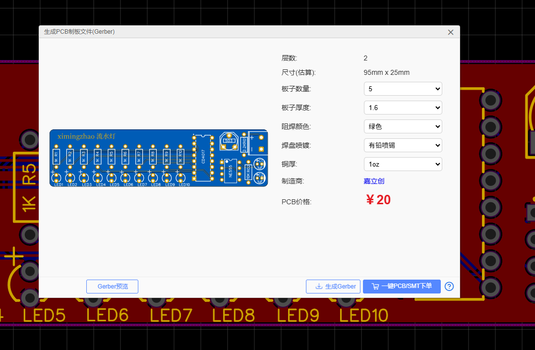
🧠 JLC EDA Workflow: Water Flow Light Project
Schematic Design
Based on the provided schematic, the Water Flow Light circuit consists of two main stages: the Pulse Generator and the Decimal Counter.
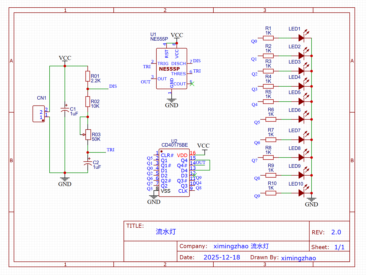
Core Chips:
- U1 (NE555): Configured in Astable Mode. It generates a continuous square wave signal.
- U2 (CD4017): A 5-stage Johnson decade counter. It receives the clock signal from the NE555 and sequentially outputs High levels to pins Q0-Q9, lighting up the LEDs one by one.
Critical Components:
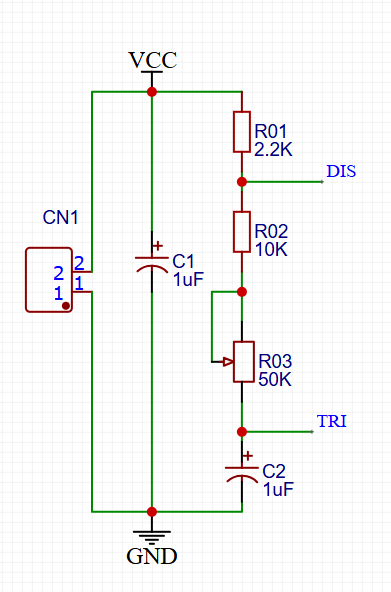
- R1 (10kΩ) & R2 (Potentiometer): These resistors, along with Capacitor C1, determine the frequency of the pulse.
- Analysis: Adjusting R2 changes the charging/discharging time of C1, thereby controlling the speed of the water flow effect.
- C1 (10μF): The timing capacitor. A larger value will slow down the flow; a smaller value will speed it up.
- LEDs (D1-D10): 10x Red LEDs (5mm or 3mm).
- Current Limiting Resistors: Typically 470Ω - 1kΩ placed in series with the LEDs to prevent burnout.
- R1 (10kΩ) & R2 (Potentiometer): These resistors, along with Capacitor C1, determine the frequency of the pulse.
Wiring Logic:
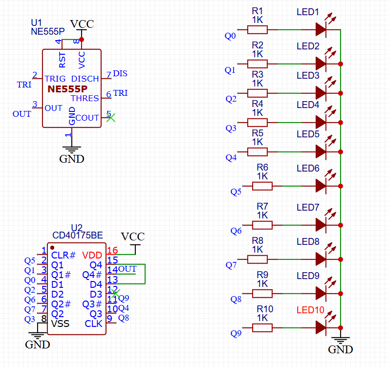
- Clock Signal: NE555 Pin 3 (Output) $\rightarrow$ CD4017 Pin 14 (CLK).
- Reset Logic: CD4017 Pin 15 (Reset) is grounded (to count continuously) or connected to Q10 (to reset after 10 steps).
PCB Layout
- Convert to PCB: Convert the schematic to PCB and define the board outline.
- Placement: Arrange LEDs in a line or circle (to simulate water flow), place chips in the center, and keep decoupling capacitors close to chip power pins.
- Routing: Use auto or manual routing. Widen power traces (e.g., 20-30mil) and keep signal traces default (e.g., 10mil).
Design Rule Check (DRC)
- Use the built-in DRC function in JLC EDA to check for Short Circuits, Clearance Errors, or Unconnected Nets.
3D Visualization
- Click the 3D preview button to check for physical component interference and view the overall appearance of the Water Flow Light.
- Click the 3D preview button to check for physical component interference and view the overall appearance of the Water Flow Light.
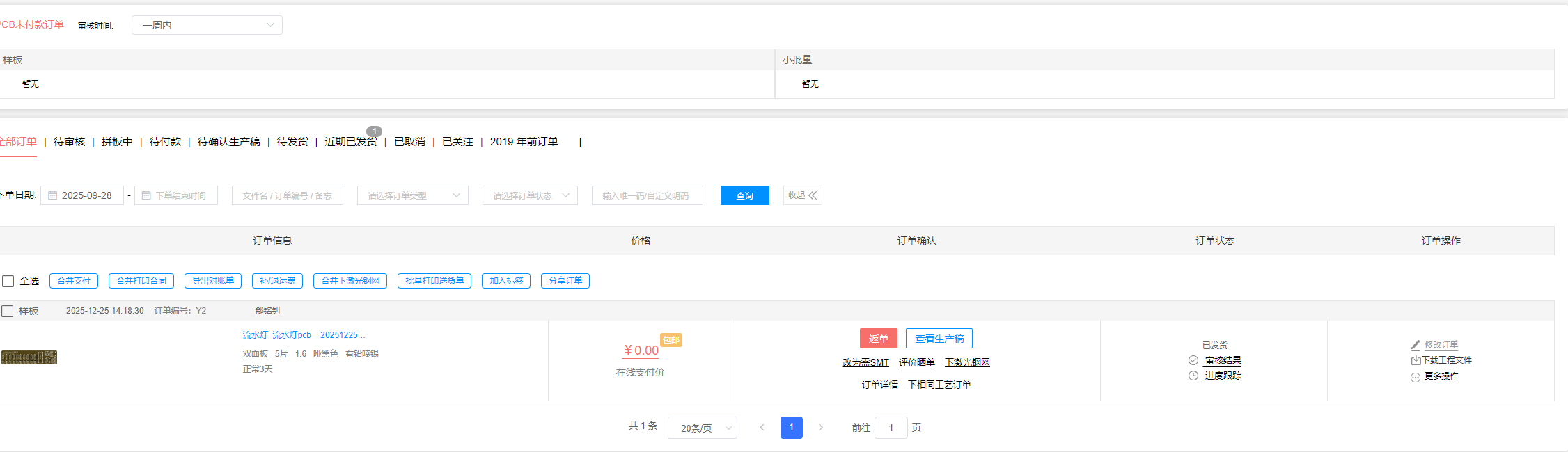
Order PCB / Export Gerber
- One-Click Order: Click "One-Click Order" to send data directly to the JLC factory for production.
- Export Gerber: Export Gerber files for local CNC milling or archiving.
⚠️ Practical PCB Considerations
Safety & Best Practices
- Check design rules (e.g., trace clearance, pad sizes).
- Ensure power/ground plane integrity for stability.
- Avoid routing errors and overlapping nets.
- Verify high‑speed design constraints if needed.
Simulation & Verification
- Circuit simulation helps catch logic errors before layout.
- 3D visualization verifies component fit and enclosure compatibility.
🧩 Extended PCB Topics
📌 High‑Speed and RF PCB Design
- Requires controlled impedance routing, differential pairs, return paths, and EMI/EMC strategies.
📌 Manufacturing and Assembly
- Panelization, solder paste stencil data, automated pick‑and‑place files.
- Working with EMS (Electronic Manufacturing Services) for production.
📌 Emerging Tools & Trends
- AI‑assisted PCB design: Startups and plugins integrating large‑language models to automate layout and error detection.
📚 Recommended Learning Resources
- KiCad tutorial series (YouTube) — beginner PCB workflow. youtube.com
- PCB design guides & rules articles for best practices. schemalyzer.com